Sometimes files of unknown formats appear on the computer, which we have not heard about before. Now we will help you deal with one of the types of such files. LAY. First you need to know that this is a file that contains an electrical schematic diagram or a printed circuit board design. Also, this extension has several varieties at the same time. They are used to calculate various types of problems, and they are created using the Sprint Layout utility.
How to run the file
Before you open .LAY, you have to understand what type of file it belongs to.
The easiest way, but not always effective, is to double-click on the file with the right mouse button. In this case, the computer itself will choose the program to open the file. But there may not be a utility on the PC that can open .LAY, so we will need to download additional software.
What software are we talking about
There are several programs working with this type of file. But before that, figure out what type of file you are going to work with. There are 5 types of .LAY files:
- Developed by Apple.
- Variant of the Tecplot program.
- Rhino 3D option.
- Template "MAME"
Now about everything in order!
Sprint Layout Utility
- a special utility from Apple. It is used on Mac OS, with which DVD projects are created. To create a project, programming knowledge is not required at all, because the program has several ready-made templates with which even a beginner can create his own DVD project without any problems. But advanced users may not use templates, but create them themselves. You can also test a DVD project without creating a disc image.
Important! The .LAY file in this case lies in the VIDEO_TS directory, but when converting the finished project to disk, it will not be written, because it belongs to the design of the project.
Tecplot program
Is a program used by engineers to create objects in flat and volumetric formats. It is used in engineering plotting and contains a wide range of functions.
LAY includes page layout, color and graphic settings. It stores information about the participant, parameters that determine the appearance of each frame and the visual layout of the project work area.
The author of the program is Tecplot.
Rhino 3D option
Rhinoceros is a commercial 3D design software NURBS. This program is used in shipbuilding, architecture, automotive, industrial design, jewelry, etc. It helps to create objects that require incredible precision. Therefore, this utility is used in the areas of CAD / CAM design and multimedia.
Advice! NURBS is used to transfer the shapes of objects in the 3D format. Therefore, it became the basis of the Rhino 3D program. NURBS generates complex 3D objects from 2D models (quads, circles, polylines, lines, etc.).
Rhino 3D stores information about the state of the layer where the 3D models are located. All models can be changed at the same time. This is done for the purpose of simultaneously changing the color or structure, and for simultaneously turning on or off layer objects.
Authors of the program:
- Robert McNeel.
- Associates.
A simple, yet very effective software package for the design and manual layout of printed circuit boards of small to medium complexity. The program is very popular among Russian radio amateurs.
The main advantage of Sprint-Layout is its intuitive interface, which includes only the most necessary tools for preparing printed circuit boards of 300 x 300 mm. The program allows you to work with two layers (conductors and markings) for each side of the board. Additional features - solder mask layer, metallization, SMD mask. The built-in router only helps you route the wires, and is not automatic. The growing library contains the most common electronic components. Sprint-Layout has the ability to export work results to the popular Excellon and Gerber formats, as well as create an HPGL file for finishing a printed circuit board on a software-controlled milling machine. The package is widely used for.
The program is hardly suitable for professionals, since its capabilities are limited by small boards with a low element density. But, thanks to its logical and understandable structure, Sprint-Layout is very easy to learn and is recommended for novice designers who do not want to waste their time on learning more complex programs.
The language of the program is German or English. Domestic enthusiasts created a fully functional Russified version of the program, which was named Sprint-Layout 6 on the network (but has nothing to do with the official 6th version, released in 2013). The interface has been redesigned for greater convenience, a large number of electronic components have been added, and compatibility with all original Sprint-Layout versions up to version 5 has been maintained.
You can read about the innovations of the 6th version of Sprint-Layout in the article:

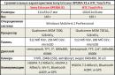
The program works stably in 32- or 64-bit operating systems Windows 98 / ME / NT / 2000 / XP / Vista / Win 7 / Win 8
Distribution of the program: Shareware (paid), price - 40 EUR
Sprint-Layout official website: http://www.abacom-online.de/uk/html/sprint-layout.html
Sprint-Layout file formats: LAY, LAY6, export to Gerber or Excellon
Download Sprint-Layout 6.0 (unofficial Russian version, actually 5.0)
Sprint-Layout is a simple program for designing both single-sided and double-sided printed circuit boards, providing almost all the necessary functions for such tasks. There is an export of files in professional formats Gerber and Excellon, used for the manufacture of boards in an industrial way, including etching and drilling.
Sprint-Layout lets you draw patches, paths, foil patches, decals, and more. You can choose a variety of shapes and sizes of elements, as well as create them yourself.
You can open the Example.LAY file in the SprintLayout directory, it contains two boards with different examples of what you can create in the program.
Download
Program sPlan - a simple and convenient tool for drawing electronic and electrical circuits, it allows you to easily transfer symbols from element libraries onto the diagram and snap them to the grid. V sPlan there's a lot instruments for drawing and editing, which make the development of circuits convenient and efficient, such as auto-numbering of elements, drawing up item lists other.
Download
Program "Schematic Builder 2003" is intended for building elementary electrical circuits. It is a good replacement for bulky counterparts. It includes about 50 vector objects (elements) of basic electrical circuits, with the exception of integrated microcircuits.
Download
QuickPic SchemCreator- raster graphic sprite-oriented editor of electrical schematic diagrams and any other pictures in bmp, gif, jpg formats.
Sprites - pictures (templates, templates, library components) in bmp, gif, jpg, ico, cur formats.
Features of the program:
The program interface is focused on quick and easy drawing of pictures (diagrams) from ready-made sprites;
Built-in editor for new sprites;
The number of "Undo" steps is limited only by the free space on your disk ;;
Magnification mode 2, 4, 8 times;
Various units of measurement: pixels, millimeters, inches;
Measuring rulers (as in MS Word);
Preview before printing;
Saving in BMP and GIF format;
Functions for convenient manipulation of sprites and image size;
New in the latest version 2.4x:
Saving a list of 10 last used sprites for quick access;
Extended possibilities of inserting text designations of radioelements;
Auto-increment function of radio element number;
Export of the list of items to a text file;
Choosing the color resolution of the picture when saving; now, by default, pictures are saved in a palette of 16 colors - this is quite enough for schemes, but if you really want to, you can choose 256 or 16 or 2 colors.
Download
Device diagram
It makes no significant difference whether we will lay the board on a piece of paper in a cage by cutting out templates of parts with leads from cardboard (although I deeply doubt that anyone will use this method in the 21st century, when every house has a computer), or we will use some kind of PCB layout program, such as sprint layout. Of course, using sprint layout will make it much easier, especially in large layouts. In both cases, first we put on the working field the part with the largest number of leads in our case it is a transistor, for example VT1, this is KT315 for us. (A link to the sprint layout manual will be provided below). And at first, when designing, your printed circuit board may resemble a schematic diagram, it's okay, I think everyone started that way. We put it, then we connect its base and emitter with tracks to the resistor R1, we also have the base VT1 connected to the output of the capacitor C1 and the output of the resistor R2. Instead of lines in the diagram, we connect the pins of the parts with a track on the printed circuit board. I also made it a rule to count the number of pins of parts connected on the circuit and on the printed circuit board, we should get the same number of connected spots.

As you can see, 3 more pins are connected to the base on our board, as well as on the diagram, on the diagram they are marked with red rings. Next, we install the transistor VT2 - this is a kt361 transistor, it is a pnp structure, but we do not care at the moment, since it also has 3 terminals and in a package exactly the same as kt315. We installed the transistor, then we connect its emitter with the second terminal R2, and the second terminal of the capacitor C1 with the collector VT2. We connect the VT2 base to the VT1 collector, install the pins on the board for connecting the BA1 speaker, we connect it with one pin to the VT2 collector, the other pin to the VT1 emitter. Here's how everything that I described looks like on the board:

We continue further, we install the LED, connect it to the BA1 pin and to the VT2 emitter. After we install the transistor VT3, this is also kt315 and connect it with a collector to the cathode of the LED, we connect the emitter VT3 to the minus of the power supply. Next, we install the resistor R4 and connect it with tracks to the base and emitter of the transistor VT3, we put the output from the base on the X1 probe. Let's see what happened on the board:

Finally, we install the last few details. Install the power switch, connecting it to the power supply plus a track from one patch and with the emitter VT2, a path from another patch connected to the switch. We connect this output of the switch with the resistor R3, and connect the second patch of the resistor to the contacts of the X2 probe.

We all love to assemble circuits, but not everyone wants and knows how to lay printed circuit boards. Most often we look for a ready-made seal on the Internet and in most cases we find it. It would seem, go ahead, etch and solder! But not everything is so rosy, because often these found seals look like this:
Not a single signed item. Complete rebus, riddle! And, like, turn on the "mosch" and stuff the elements, because the diagram is at hand. But the program was created to make life easier for us, and not vice versa.
Therefore, I will briefly, from the very beginning, tell you how to approach the layout of the board in Sprint-Layout, so that you do not need to guess later what kind of detail I put in here. Let's get it right right away!
You cannot cover everything in one small article, I will go through some of the main points. So, we create a new project, set the name of the board and the estimated size (it can be easily adjusted later).

Don't forget to choose a suitable work mesh.

For small projects with large elements, a mesh of 1.27 mm is suitable, for more advanced and dense 0.635 mm, and so on. Elements and tracks will be placed with reference to the nodes of this grid. You can make a grid for Soviet parts: 2.5 mm or 1 mm.

Be sure to understand the layer system in the program, understand how everything works, use the photo view.

Make labels on layers for labels, and tracks and polygons on layers for copper, etc.
The archive contains help programs in Russian.
We start adding details to the board. At this stage, the values of "Type" and "Denomination" should not be confused, later I will tell you why.

Enter the values, adjust the font size to taste, click OK.

We see the element with the marking. Now we can distribute and "seal" our markings.
We select the denomination and drag it with the mouse to the desired place. Before that, you need to reduce the size of the grid to an acceptable level.

That's better.

Now move the element designation closer. If necessary, you can rotate it by selecting it before.

Further, so as not to suffer so much with each element, we simply copy it and change the data in the element's properties.

Our board is already quite ready to manufacture, but why do we need to overload the solution with excess copper?
There is no need! We will minimize the area of copper to be vented. To do this, select all the elements on the board and press the "Metallization" button at the bottom of the program window and change the value to an acceptable one, for example 0.5 mm.

Everything is fine, but some legs can and sometimes even need to be planted on a metallized area. There is nothing difficult.

Select the required legs and change the metallization offset value to 0. That's it, now the leg is on the earth bus.

And if you need a thermal barrier to facilitate soldering on large polygons? Select the path drawing and draw the thermal barrier.

This is the simplest and most obvious way. But you can also use the built-in capabilities of the program to create thermal barriers. Highlight the pad you want and study the menu on the right.

Check the "Thermal barrier" checkbox and adjust the direction and width of the "bridges" of the barrier. It is very convenient that many sites can be configured at once. The thermal barrier function works only on the switched on automatic landfill. Not supported by all versions of Sprint-Layout. Use fresh.
Everything is drawn, we can admire the result by pressing the "photoview" button.

A nuance - you can edit the size of the labels of the elements separately, for this, select the "victim" and press the properties button on the right. The settings are pretty extensive. However, it is best to set all decals in the same style.

It was the turn of the "cosmetics". So that all the drawings of the elements on the board have a uniform appearance and line thickness, do the following:
1.select the layer with the marking of the elements;
2. turn off the track layer;
3. select everything (ctrl + A);
4. adjust the thickness of the lines of all elements at the same time;
5. Activate the tracks layer again.


The beauty! By the way, do not forget to adjust the colors of the layers in the program to all taste, to whom my palette seemed gloomy.
Now let's recall the beginning of the article and find out why you shouldn't enter the nominal value of an element in the field for its type. It's simple, it turns out that when we add elements, we have already formed a list of elements!
Of course, the more correct practice is the primacy of the circuit in the project, then the creation of the list of elements is the business of the program for drawing the circuits. In the set of programs from ABACOM it is sPLAN.
Editorial note

It remains only to buy according to the list and get a beautiful home-made board as a result. And people are not ashamed to show such a drawing on the forum, and there will be no unnecessary questions about the board.
Files
And here is the Russian help for Sprint-Layout and an excellent free book of our comrade Mikhail Tsarev (Tsoy73):▼ 🕗 27/12/16 ⚖️ 2.14 Mb ⇣ 168